
MC14511B/D BCD–to–seven segment latch/decoder/driver is constructed with complementary MOS (CMOS) enhancement mode devices and NPN bipolar output drivers in a single monolithic structure. The circuit provides the functions of a 4–bit storage latch, an 8421 BCD–to–seven segment decoder, and an output drive capability. Lamp test (LT), blanking (BI), and latch enable (LE) inputs are used to test the display, to turn–off or pulse modulate the brightness of the display, and to store a BCD code, respectively. It can be used with seven–segment light–emitting diodes (LED), incandescent, fluorescent, gas discharge, or liquid crystal readouts either directly or indirectly. Applications include instrument (e.g., counter, DVM, etc.) display driver, computer/calculator display driver, cockpit display driver, and various clock, watch, and timer uses.
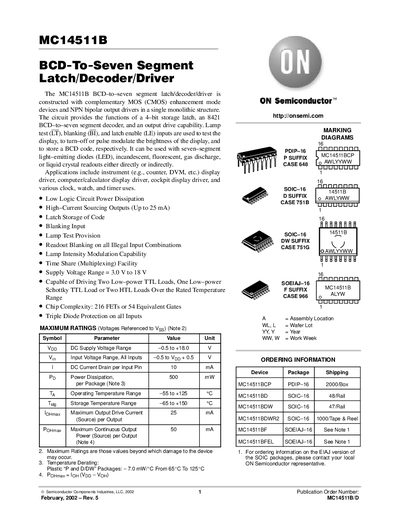
The MC14511B provides a 4‑bit storage latch, a 8421 BCD‑to‑seven‑segment decoder, and high‑current output drivers in a single CMOS monolithic package. It is suitable for instrument displays, calculators, cockpit displays, clocks, watches and timers, and can drive LED, incandescent, fluorescent, gas‑discharge or LCD readouts.
Key specifications include a supply voltage range of 3.0 V to 18 V, maximum output drive current of 25 mA, power dissipation of 500 mW per package, and an operating temperature range of –55 °C to +125 °C. The device is offered in PDIP‑16 and SOIC‑16 (EIAJ) packages with detailed electrical and switching characteristics provided.
| Supply Voltage Range | 3.0 V to 18 V |
|---|---|
| Maximum Output Drive Current | 25 mA |
| Power Dissipation per Package | 500 mW |
| Operating Temperature Range | -55 °C to +125 °C |
| Input Pin Current Drain | 10 mA |
| Package Type (PDIP) | PDIP‑16 |
| Package Type (SOIC) | SOIC‑16 |
The MC14511B can source up to 25 mA per output pin.
It operates from 3.0 V up to 18 V.
The device is offered in PDIP‑16 and SOIC‑16 (EIAJ) packages.