
The LMK03000 family of precision clock conditioners combines the functions of jitter cleaning/reconditioning, multiplication, and distribution of a reference clock. The devices integrate a Voltage Controlled Oscillator (VCO), a high performance Integer-N Phase Locked Loop (PLL), a partially integrated loop filter, and up to eight outputs in various LVDS and LVPECL combinations. The VCO output is optionally accessible on the Fout port. Internally, the VCO output goes through a VCO Divider to feed the various clock distribution blocks. Each clock distribution block includes a programmable divider, a phase synchronization circuit, a programmable delay, a clock output mux, and an LVDS or LVPECL output buffer. This allows multiple integer-related and phase-adjusted copies of the reference to be distributed to eight system components. The clock conditioners come in a 48-pin LLP package and are footprint compatible with other clocking devices in the same family.
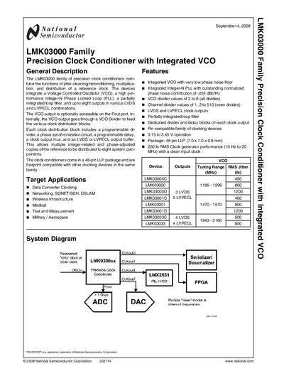
The LMK03000 family combines jitter cleaning, multiplication, and distribution functions in a single device. It integrates a VCO, an Integer‑N PLL, and up to eight LVDS or LVPECL clock outputs with programmable delay and muxing, making it suitable for networking, wireless, medical, test, and aerospace applications.
The devices are offered in a 48‑pin LLP package (7.0 × 7.0 × 0.8 mm) and feature pin‑compatible families, a partially integrated loop filter, and a range of programmable divider values. Detailed electrical characteristics, absolute maximum ratings, and clock‑distribution specifications are provided for design reference.
| Phase noise contribution | -224 dBc/Hz |
|---|---|
| Power supply voltage (operating) | 3.15 V – 3.45 V |
| Package | 48‑pin LLP (7.0 × 7.0 × 0.8 mm) |
The device operates with a supply voltage between 3.15 V and 3.45 V.