
The DP83848I is a robust fully featured 10/100 single port Physical Layer device offering low power consumption, including several intelligent power down states. These low power modes increase overall product reliability due to decreased power dissipation. Supporting multiple intelligent power modes allows the application to use the absolute minimum amount of power needed for operation. In addition to low power, the DP83848I is optimized for cable length performance far exceeding IEEE specifications. The DP83848I includes a 25MHz clock out. This means that the application can be designed with a minimum of external parts, which in turn results in the lowest possible total cost of the solution. The DP83848I easily interfaces to twisted pair media via an external transformer and fully supports JTAG IEEE specification 1149.1 for ease of manufacturing. Additionally both MII and RMII are supported ensuring ease and flexibility of design. The DP83848I features integrated sublayers to support both 10BASE-T and 100BASE-TX Ethernet protocols, which ensures compatibility and interoperability with all other standards based Ethernet solutions. The DP83848I is offered in a small form factor
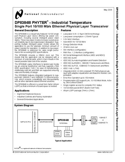
The DP83848I is a robust 10/100 Mb/s Ethernet physical layer device offering low power consumption, multiple power‑down states, and an integrated 25 MHz clock output, reducing external component count. It supports MII, RMII and SNI interfaces, auto‑MDIX, and includes programmable LED functions for link and activity indication.
The datasheet provides detailed pin descriptions, configuration options, functional block diagrams, electrical specifications, package dimensions (48‑pin LQFP, 7 mm × 7 mm), and a complete register map for software control and diagnostics.
| Clock output | 25 MHz |
|---|---|
| Typical power consumption | < 270 mW |
| Package | 48‑pin LQFP (7 mm × 7 mm) |
| Operating voltage | 3.3 V |
| Supported interfaces | MII, RMII, SNI |
| Auto‑MDIX support | Enabled for 10/100 Mb/s |
The DP83848I provides a 25 MHz clock output.
Typical power consumption is less than 270 mW.
It is supplied in a 48‑pin LQFP package measuring 7 mm × 7 mm.
The device supports MII, RMII, and SNI interfaces.