
The DS91M040 is a quad M-LVDS transceiver designed for driving / receiving clock or data signals to / from up to four multipoint networks.
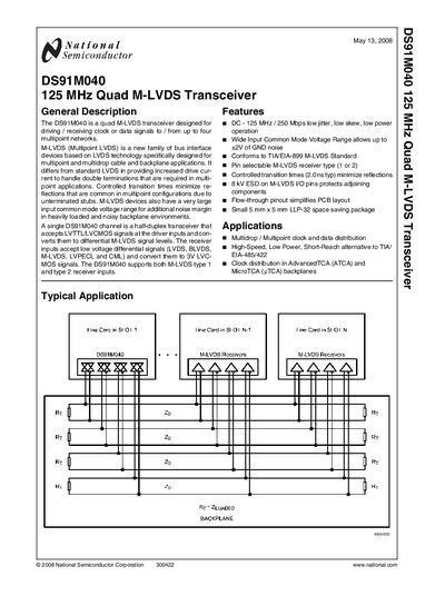
The DS91M040 is a quad M‑LVDS transceiver designed for driving and receiving clock or data signals across up to four multipoint networks. It supports LVTTL/LVCMOS driver inputs and converts them to differential M‑LVDS levels, while the receiver accepts LVDS, BLVDS, M‑LVDS, LVPECL and CML signals.
Key features include 125 MHz (250 Mbps) operation, wide input common‑mode range (+2 V GND noise), pin‑selectable receiver types, low jitter and skew, 8 kV ESD protection, and a compact 5 mm × 5 mm LLP‑32 package. The document provides ordering information, pin descriptions, electrical and switching characteristics, test circuits, and mechanical dimensions.
| Maximum operating frequency | 125 MHz |
|---|---|
| Data rate | 250 Mbps |
| Supply voltage range | -0.3 V to +4 V |
| ESD protection (HBM) | 8 kV |
| Package | LLP‑32, 5 mm × 5 mm |
The DS91M040 supports up to 125 MHz operation, which corresponds to a data rate of 250 Mbps.
The DE pin is the driver enable pin; the driver is disabled when DE is low and enabled when DE is high.
The M‑LVDS I/O pins are rated for 8 kV ESD protection (Human Body Model).
The device is offered in an LLP‑32 package measuring approximately 5 mm × 5 mm.