
The Si9912 is a dual MOSFET high-speed driver with break-before-make. It is designed to operate in high frequency dc-dc switchmode power supplies. The high-side driver is bootstrapped to handle the high voltage slew rate associated with “floating” high-side gate drivers. Each driver is capable of switching a 3000-pF load with 60-ns propogation delay and 25-ns transition time. The Si9912 comes with an internal break-before-make feature to prevent shoot-through current in the external MOSFETs. A shutdown pin is used to enable the driver. When disabled, the quiescent current of the driver is less than 5 μA. The Si9912 is available in both standard and lead (Pb)-free, 8-pin SOIC packages for operation.
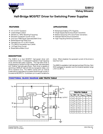
The Si9912 is a dual MOSFET high‑speed driver designed for high‑frequency switching power supplies. It operates from a 4.5‑55 V supply, provides up to 1 A peak drive current, and includes features such as undervoltage lockout, shutdown control, and a break‑before‑make circuit to prevent shoot‑through.
The device is supplied in SO‑8 and lead‑free SOIC packages, supports a wide temperature range (‑40 °C to 125 °C), and is intended for applications like desktop CPU supplies, mobile computing power converters, and standard‑synchronous buck converters. Layout guidelines emphasize short, low‑inductance traces and close decoupling to achieve nanosecond switching performance.
| Low Side Driver Supply Voltage (Vop) max | 7.0 V |
|---|---|
| Input Voltage on IN (VIN) range | -0.3 to Vpp +0.3 |
| Shutdown Pin Voltage (Vep) range | -0.3 to Vop +0.3 V |
| Bootstrap Voltage max | 35.0 V |
| Operating Junction Temperature Range | -40 °C to 125 °C |
| Power Dissipation | 830 mW |
| Peak Output Drive Current | 1 A |
The Si9912 operates from 4.5 V up to 55 V supply voltage.
It can deliver up to 1 A of peak output drive current.
Yes, it has an internal break‑before‑make circuit to prevent shoot‑through when switching MOSFETs.
The shutdown pin is active low; when low it turns off both high‑ and low‑side MOSFETs.