
The ADC08L060 is a low-power, 8-bit, monolithic analog-to-digital converter with an on-chip track-and-hold circuit. Optimized for low cost, low power, small size, and ease of use, this product operates at conversion rates of 10 MSPS to 60 MSPS while consuming just 0.65 mW per MHz of clock frequency, or 39 mW at 60 MSPS. Raising the PD pin puts the ADC08L060 into a Power Down mode where it consumes about 1 mW. The unique architecture achieves 7.6 Effective Bits. The ADC08L060 is resistant to latch-up and the outputs are short-circuit proof. The top and bottom of the ADC08L060s reference ladder are available for connections, enabling a wide range of input possibilities. The digital outputs are TTL/ CMOS compatible with a separate output power supply pin to support interfacing with 1.8V to 3V logic. The output coding is straight binary and the digital inputs (CLK and PD) are TTL/ CMOS compatible. The ADC08L060 is offered in a 24-lead plastic package (TSSOP) and is specified over the industrial temperature range of −40°C to +85°C.
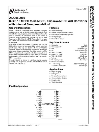
The ADCO8L060 is a low‑power, 8‑bit monolithic ADC with an on‑chip track‑and‑hold circuit. It operates from 10 MSPS up to 60 MSPS while consuming only 0.65 mW per MHz of clock frequency (≈39 mW at 60 MSPS). The device features single‑ended input, internal sample‑and‑hold, power‑down mode (~1 mW), and TTL/CMOS‑compatible digital outputs.
Key specifications include a 24‑lead TSSOP package, an industrial temperature range of –40 °C to +85 °C, a latency of 5 clock cycles, and a conversion rate of 10‑60 MSPS. Typical applications are digital imaging, set‑top boxes, portable instrumentation, communication systems, X‑ray imaging, and Viterbi decoders.
| Conversion Rate | 10 MSPS to 60 MSPS |
|---|---|
| Power Consumption (typical) | 0.65 mW per MHz of clock (≈39 mW at 60 MSPS) |
| Package | 24‑lead TSSOP |
| Operating Temperature Range | -40 °C to +85 °C |
| Latency | 5 Clock Cycles |
It consumes about 39 mW at 60 MSPS (0.65 mW per MHz of clock frequency).
The device operates from –40 °C to +85 °C.
The converter has a latency of 5 clock cycles.
It is offered in a 24‑lead TSSOP package.