
The DS90CF363 is a 3.3V LVDS transmitter that converts 21 bits of CMOS/TTL data into three LVDS data streams. It supports clock frequencies from 20 to 65 MHz and resolutions up to VGA, SVGA, XGA, etc. The narrow bus design reduces cable size and cost, while the low EMI LVDS devices ensure reliable transmission.
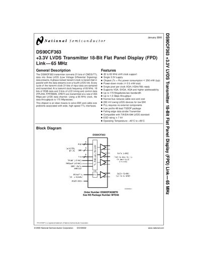
The DS90CF363 transmitter converts 21 bits of CMOS/TTL data into three LVDS data streams and a fourth LVDS clock link. It operates with a 3.3 V supply, supports shift clocks from 20 MHz to 65 MHz, and delivers up to 170 Mbytes/sec (≈1.3 Gbps) of data throughput.
The device is offered in a 48‑lead TSSOP package, features low power consumption (<250 mW typical), and includes a power‑down mode with less than 0.5 mW total draw. It complies with the TIA/EIA‑644 LVDS standard and provides a 290 mV LVDS swing for low EMI.
| Operating Temperature | -40 °C to +85 °C |
|---|---|
| Maximum Data Rate per LVDS Channel | 455 Mbit/s |
The device operates from –40 °C up to +85 °C.