
The ADF4002 frequency synthesizer is used to implement local oscillators in the upconversion and downconversion sections of wireless receivers and transmitters. It features a 400 MHz bandwidth, 2.7V to 3.3V power supply, separate charge pump supply for extended tuning voltage in 3V systems, programmable charge pump currents, 3-wire serial interface, analog and digital lock detect, hardware and software power-down mode, and a 104 MHz phase detector.
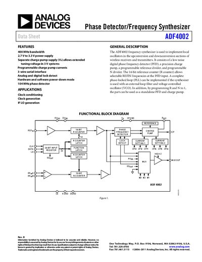
The ADF4002 is a 400 MHz bandwidth phase detector/frequency synthesizer designed for clock conditioning, clock generation, and IF LO generation in wireless receivers and transmitters. It features a low‑noise digital phase‑frequency detector, programmable charge pump, 14‑bit reference counter, and 13‑bit N‑counter, with a 3‑wire serial interface and both analog and digital lock detection.
The datasheet includes detailed specifications such as supply voltage ranges, RF and reference input characteristics, timing parameters, absolute maximum ratings, thermal data, pin configurations for TSSOP and LFCSP packages, and typical performance graphs. Ordering information and package dimensions are also provided.
| RF Input Frequency range | 5 MHz – 400 MHz |
|---|---|
| REFIN Input Frequency range | 20 MHz – 300 MHz |
| AVDD supply voltage | 2.7 V – 3.3 V |
| Phase Detector Frequency | 104 MHz |
| Charge Pump High Current | 5 mA |
| Operating Temperature Range (Industrial) | -40 °C to +85 °C |
The AVDD (analog power supply) must be between 2.7 V and 3.3 V.
The device is rated for an industrial temperature range of –40 °C to +85 °C.