
The document describes the features and characteristics of the ADF4001 200 MHz Clock Generator PLL. It has a bandwidth of 200 MHz, a power supply range of 2.7 V to 5.5 V, programmable charge pump currents, and a 3-wire serial interface. The product is suitable for clock generation, low frequency PLLs, and low jitter clock applications.
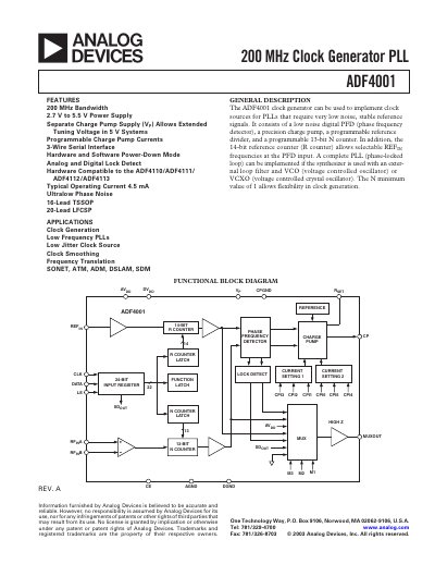
The ADF4001 is a low‑noise clock generator PLL that includes a digital phase‑frequency detector, precision charge pump, programmable reference divider and a 13‑bit N counter. It supports a 200 MHz output frequency and offers a 3 V to 5.5 V supply range with programmable charge‑pump currents.
The document provides detailed electrical specifications, timing characteristics, pin functions for both TSSOP and LFCSP packages, and typical performance graphs such as phase‑noise and output power. It also includes an ordering guide and recommended ESD handling procedures.
| Maximum Output Frequency | 200 MHz |
|---|---|
| Supply Voltage Range | 2.7 V to 5.5 V |
| Typical Operating Current | 4.5 mA |
| Phase Noise Floor | –161 dBc/Hz @ 200 kHz |
| RSET Resistor Value | 4.7 kΩ |
| Package Options | 16‑lead TSSOP, 20‑lead LFCSP |
The device operates from 2.7 V to 5.5 V supply voltage.
The TSSOP package has 16 pins.
Typical operating current is 4.5 mA.
The phase‑noise floor is –161 dBc/Hz at a 200 kHz offset.