
The AP1212 is a Diodes Incorporated dual USB high side power switch that complies with USB specifications, has dual independent switch control, 2.7V to 5.5V input voltage, 500mA minimum continuous current per port, 110mΩ typical on-resistance, 1.25A maximum short circuit current limit, independent open-drain fault flag pins, 110μA typical on-state supply current, 1μA typical off-state supply current, output can be forced higher than input (off-state), thermal shutdown, 2.4V typical under voltage lockout (UVLO), 1ms turn-on (soft-start) and fast turn-off, enable active-high (H) or active-low (L), SOP-8L: Available in “Green” Molding Compound (No Br, Sb), Lead Free Finish/RoHS Compliant (Note 1), USB hubs, Hot plug-in power supplies, battery-charger circuits
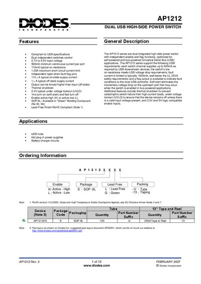
The AP1212 series provides dual independent high‑side switches optimized for self‑powered and bus‑powered USB applications. Each channel can deliver up to 500 mA, features a typical on‑resistance of 110 mΩ, and includes open‑drain fault‑flag pins to signal over‑current, UVLO, or thermal shutdown conditions.
The device operates from a 2.7 V to 5.5 V supply, offers active‑high or active‑low enable inputs, and incorporates thermal shutdown at 140 °C with a 10 °C hysteresis. Recommended external components include bypass capacitors (0.1 µF–1 µF) and ferrite beads for EMI suppression during hot‑plug events.
| Input voltage range | 2.7 V to 5.5 V |
|---|---|
| Typical on‑resistance | 110 mΩ |
| Continuous load current per output | 0.6 A |
| Turn‑on delay (RL=10 Ω) | 30 µs |
| Thermal shutdown threshold | 140 °C (hysteresis 10 °C) |
| Fault flag voltage | +7 V |
| Enable input threshold (low) | 0.8 V to 1.7 V |
Each switch channel supplies up to 500 mA as required by USB downstream devices.
Fault conditions are signaled by open‑drain fault‑flag pins (FLG1, FLG2) that are pulled low when an over‑current, UVLO, or thermal shutdown occurs.
The enable input can be active‑high (H) or active‑low (L); low‑level threshold is 0.8 V–1.7 V and high‑level threshold is about 2.4 V.
A 0.1 µF to 1 µF bypass capacitor from IN to GND is strongly recommended to control supply transients.