
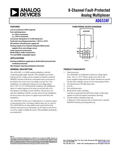
The ADG528F is an 8‑channel CMOS analog multiplexer that provides fault‑protected operation. It uses a series n‑channel, p‑channel, n‑channel MOSFET structure to protect both the device and the signal source during over‑voltage or power‑loss conditions. All switches turn off when the supply is removed, and leakage currents remain in the nanoampere range.
Key specifications include a typical on‑resistance of 300 Ω, fault protection from –40 V to +55 V, fast switching times (250 ns), and low power dissipation (≤3.3 mW). The device is addressed via three binary inputs (A0‑A2) and includes on‑chip latches for microprocessor interfacing. Pin configurations, timing diagrams, absolute maximum ratings and ordering information are provided in the following sections.
| Typical on‑resistance (RON) | 300 Ω |
|---|---|
| Maximum on‑resistance (RON) | 400 Ω |
| Fault and over‑voltage protection range | –40 V to +55 V |
| Source off leakage current (IS Off) | ±0.02 nA typical |
| Supply current (IDD) | 0.1 mA max |
| Maximum supply voltage difference (VDD to VSS) | 44 V |
| Over‑voltage rating with power off | –40 V to +55 V |
The device can withstand continuous over‑voltage inputs from –40 V to +55 V.
Its typical on‑resistance is 300 Ω.
It has eight single channels that are selected by the 3‑bit address lines A0, A1 and A2.