
NTLJD3119C/D is a combination of N-MOSFET and P-MOSFET, its working voltage is 20V/-20V, rated current is 4.6A/-4.1A, and it adopts WDFN package. The combination adopts leading edge trench technology, with low on resistance, low gate threshold voltage, low package height and other features. It can be widely used in synchronous DC-DC conversion circuits, load/power management and other fields.
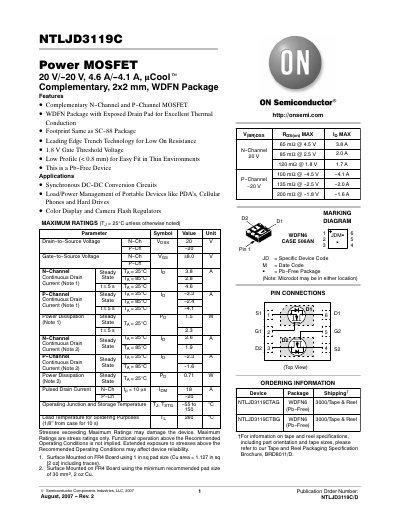
The NTLJD3119C/DNTLJD3119C is a complementary pair of N‑channel and P‑channel power MOSFETs offered in a 2 × 2 mm WDFN6 package with an exposed drain pad for excellent thermal conduction. It is designed for low‑profile applications such as portable device power management and synchronous DC‑DC conversion circuits.
Key electrical characteristics include a 20 V drain‑to‑source rating for the N‑channel and –20 V for the P‑channel, continuous drain currents of 3.8 A (N) and –3.3 A (P) at 25 °C, and a typical on‑resistance below 2 Ω. The device is Pb‑free and supports soldering lead temperatures up to 260 °C for 10 s.
| Drain-to-Source Voltage (N‑Channel) | 20 V |
|---|---|
| Power Dissipation (continuous) | 1.5 W |
The N‑channel version is rated for 20 V and the P‑channel version for –20 V drain‑to‑source voltage.