
This file is the M74HC367 datasheet
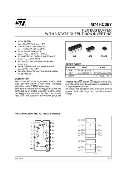
The M74HC367 is a high‑speed CMOS hex bus buffer with three‑state non‑inverting outputs. It contains six buffers; four are enabled by G1 and two by G2, with all inputs protected against static discharge and transient voltages.
The document lists absolute maximum ratings, recommended operating conditions, DC and AC electrical characteristics, test circuits, waveform examples, and mechanical dimensions for DIP‑16, SO‑16, and TSSOP‑16 packages.
| Supply Voltage Range | 2 V to 6 V |
|---|---|
| Typical Propagation Delay | 9 ns |
| Maximum Output Current (Low) | 35 mA |
| Maximum Power Dissipation | 500 mW at 65 °C |
The device operates from 2 V to 6 V.
It contains six buffers, four controlled by G1 and two by G2.
Pins G1 and G2 are 3‑state output enable inputs.
The maximum power dissipation is 500 mW at 65 °C (derated to 300 mW at higher temperatures).