
This datasheet provides detailed information on the features and characteristics of the STMicroelectronics STB60NF06/STB60NF06-1 N-channel 60V-0.014Ω-60A D2PAK/I2PAK STripFET™ II Power MOSFET.
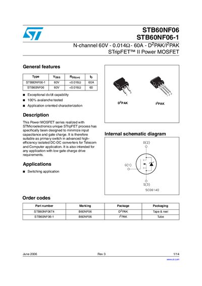
The STB60NF06 is a 60 V N‑channel power MOSFET designed with STMicroelectronics' STripFET process to achieve low input capacitance and gate charge, making it suitable for switching applications in telecom, computer, and other low‑gate‑charge driven circuits.
The document lists absolute maximum ratings, thermal data, avalanche characteristics, and detailed electrical characteristics such as on‑resistance, gate charge, and capacitances. Test circuits and characteristic curves illustrate switching performance and diode recovery behavior, and packaging information for DPAK and TO‑220 variants is provided.
| Drain‑source voltage (VDS) | 60 V |
|---|---|
| Continuous drain current (ID) at 25 °C | 60 A |
| Total power dissipation (PD) | 110 W |
| Thermal resistance junction‑case (RθJC) | 1.36 °C/W |
| Single‑pulse avalanche energy (EAS) | 460 mJ |
| Input capacitance (Ciss) | 1810 pF |
The device is rated for a maximum drain‑source voltage of 60 V.
It can conduct up to 60 A continuously at 25 °C.
The MOSFET can dissipate up to 110 W at 25 °C.