
This document describes the features and characteristics of the TL072, TL072A, and TL072B low noise JFET dual operational amplifiers, including wide common-mode and differential voltage range, low input bias and offset current, low noise, output short-circuit protection, high input impedance JFET input stage, low harmonic distortion, etc.
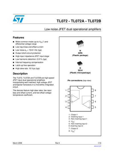
The TLO72 family comprises three low‑noise JFET dual operational amplifiers (TLO72, TLO72A, TLO72B). They feature high slew rates, low input bias and offset currents, wide common‑mode range, and internal frequency compensation. The devices are offered in plastic SO‑8 and DIP‑8 packages.
The handbook provides detailed pin‑out diagrams, absolute maximum ratings, operating conditions, and electrical characteristics such as gain, offset voltage, slew rate, and total harmonic distortion. Revision history and legal notices are included at the end of the document.
| Supply voltage range | 6 V to 36 V |
|---|---|
| Slew rate (typical) | 16 V/µs |
| Input offset voltage (typical) | 3 mV (TLO72B) |
The devices can operate with a supply voltage from 6 V up to 36 V.
The typical slew rate is 16 V/µs.
The TLO72B has a typical input offset voltage of 3 mV.