
This document introduces a self-protected field-effect transistor (FET) product with temperature and current limit features. The product utilizes ON Semiconductor's latest MOSFET technology process to achieve the lowest possible on-resistance per silicon area while incorporating smart features. Integrated thermal and current limits work together to provide short circuit protection. The product also features an integrated drain-to-gate clamp that enables it to withstand high energy in the avalanche mode and provides additional safety margin against unexpected voltage transients. Electrostatic discharge (ESD) protection is provided by an integrated gate-to-source clamp.
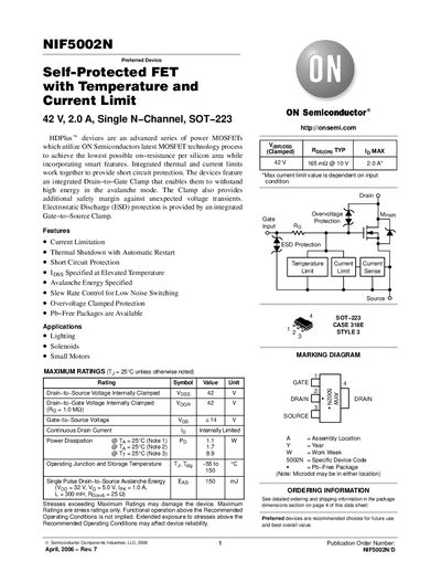
The NIF5002N is a 42 V, 2 A single N‑channel MOSFET in a SOT‑223 package that incorporates integrated thermal and current limits, a drain‑to‑gate clamp for avalanche protection, and ESD protection via a gate‑to‑source clamp. It is designed for lighting, solenoids, and small‑motor applications and offers features such as short‑circuit protection, thermal shutdown with automatic restart, and slew‑rate control for low‑noise switching.
Maximum ratings include a 42 V drain‑to‑source voltage (internally clamped), 2 A continuous drain current, 14 W typical power dissipation, and a 150 mJ avalanche energy rating. The device is supplied in Pb‑free SOT‑223 (TO‑261) packages with detailed ordering information and package dimensions provided for tape‑and‑reel handling.
| Drain‑to‑Source Voltage (V_DSS) | 42 V (internally clamped) |
|---|---|
| Continuous Drain Current (I_D) | 2.0 A (max) |
| Power Dissipation (P_D) | 14 W (typical at 25 °C) |
| On‑Resistance (R_DS(on)) | 165 mΩ (typical at 25 °C) |
| Junction‑to‑Ambient Thermal Resistance (RθJA) | 114 °C/W (steady state) |
| Avalanche Energy (E_AS) | 150 mJ |
| ESD Human Body Model Rating | 4000 V |
The device is rated for a maximum drain‑to‑source voltage of 42 V, internally clamped.
Yes, it has an integrated current limit that restricts the drain current to a maximum of 2.0 A.
It is offered in a SOT‑223 (TO‑261) case 318E‑04 package.
The temperature limit for turn‑off is 150 °C at a gate voltage of 5 V (or 10 V), with reset temperatures around 135 °C.