
The MAX5590–MAX5595 are octal, 12/10/8-bit, voltage-output digital-to-analog converters (DACs) with buffered outputs and a 3µs maximum settling time at the 12-bit level. The DACs operate from a +2.7V to +5.25V analog supply and a separate +1.8V to +5.25V digital supply. The 20MHz 3-wire serial interface is compatible with SPI™, QSPI™, MICROWIRE™, and digital signal processor (DSP) protocol applications. Multiple devices can share a common serial interface in direct-access or daisy-chained configuration. The MAX5590–MAX5595 provide two multifunction, user-programmable, digital I/O ports. The externally selectable power-up states of the DAC outputs are either zero scale, midscale, or full scale. Software-selectable FAST and SLOW settling modes decrease settling time in FAST mode, or reduce supply current in SLOW mode. The MAX5590/MAX5591 are 12-bit DACs, the MAX5592/MAX5593 are 10-bit DACs, and the MAX5594/MAX5595 are 8-bit DACs. The MAX5590/MAX5592/MAX5594 provide unity-gain-configured output buffers, while the MAX5591/MAX5593/MAX5595 provide force-sense-configured output buffers. The MAX5590–MAX5595 are specified over the extended -40°C to +85°C temperature range, and are available in space-saving 24-pin and 28-pin TSSOP packages.
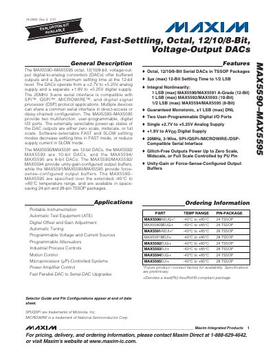
The MAX5590‑MAX5595 family are octal voltage‑output digital‑to‑analog converters offering 12‑, 10‑, or 8‑bit resolution with buffered outputs and a maximum 3 µs settling time. They operate from a +2.7 V to +5.25 V analog supply and a separate +1.8 V to +5.25 V digital supply, and support SPI, QSPI, MICROWIRE, and DSP‑compatible serial interfaces.
These devices are specified for -40 °C to +85 °C operation and are available in 24‑pin and 28‑pin TSSOP packages. Applications include portable instrumentation, automatic test equipment, programmable voltage/current sources, industrial process control, motion control, and microprocessor‑controlled systems.
| Resolution | 12‑bit (MAX5590/5591), 10‑bit (MAX5592/5593), 8‑bit (MAX5594/5595) |
|---|---|
| Maximum Settling Time | 3 µs (12‑bit) |
| Power‑Supply Rejection Ratio (PSRR) | 200 µV/V (full‑scale output, AVDD = 2.7‑5.25 V) |
| Operating Temperature Range | -40 °C to +85 °C |
| Package Types | 24‑pin TSSOP, 28‑pin TSSOP |
| Analog Supply Voltage (AVDD) | 2.70 V to 5.25 V |
| Digital Supply Voltage (DVDD) | 1.8 V to 5.25 V |
| Maximum Current per Pin | ±50 mA |
The devices support a 20 MHz 3‑wire serial interface compatible with SPI, QSPI, MICROWIRE, and DSP protocols.
The DAC outputs can be configured to power up at zero scale, midscale, or full scale.
Each pin can handle up to ±50 mA of current.