
HCF40107B is a monolithic integrated circuit fabricated in MOS technology, which can be used for dual 2-input NAND buffer/driver. This device features a wired-OR capability and high output sink current capability.
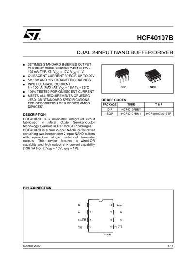
The HCF40107B is a dual 2‑input NAND buffer/driver available in DIP and SOP packages. It features open‑drain outputs with wired‑OR capability and a high output sink current of 136 mA at 10 V.
The document lists absolute maximum ratings, recommended operating conditions, DC and dynamic electrical characteristics, and example circuits such as line‑driver and motor‑controller applications. Mechanical dimensions for the SO‑8 package are also included.
| Output sink current (typ) | 136 mA at Vpp=10 V, Vpg=1 V |
|---|---|
| Supply voltage range | -0.5 V to +22 V |
| Propagation delay (typ) | 100 ns at 5 V |
| Input leakage current (max) | 100 nA at Vpp=18 V |
The device can be powered from –0.5 V up to +22 V.
It can sink up to 136 mA when Vpp is 10 V and Vpg is 1 V.
The typical propagation delay is about 100 ns at a 5 V supply.
The input leakage current is limited to 100 nA (max) at Vpp = 18 V.