
This datasheet provides the maximum ratings and technical specifications of SPP20N60C2, SPB20N60C2, SPA20N60C2 devices.
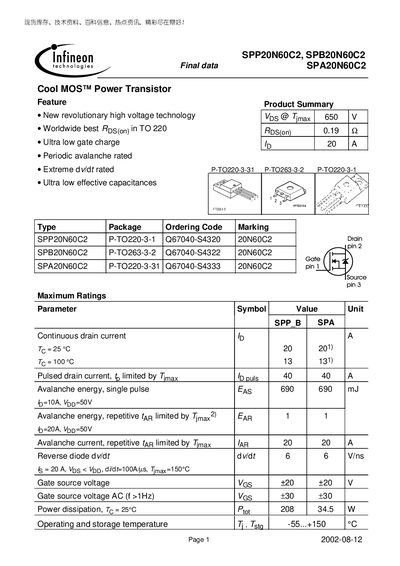
The Infineon SPP20N60C2 series are high‑voltage, low‑gate‑charge power MOSFETs offered in TO‑220, TO‑263 and FullPAK packages. The document provides detailed electrical, thermal and switching characteristics, along with maximum ratings and safe operating area curves.
Key parameters include a continuous drain current of 20 A, a drain‑source breakdown voltage of 600 V, ultra‑low gate charge, and low on‑state resistance. Thermal resistance values, transient thermal impedance, and switching loss data are also listed to aid designers in thermal management and efficiency calculations.
| Continuous drain current (Id) at 25 °C | 20 A |
|---|---|
| Drain‑source breakdown voltage (Vds) | 600 V |
| Gate threshold voltage (Vgs(th)) | 3.5 V – 5.5 V |
| On‑state resistance (Rds(on)) | 0.16 Ω – 0.19 Ω |
| Power dissipation (Pd) at 25 °C | 34.5 W |
The maximum continuous drain current is 20 A at a case temperature of 25 °C.
The MOSFETs are rated for a drain‑source breakdown voltage of 600 V.
Typical on‑state resistance ranges from 0.16 Ω to 0.19 Ω depending on temperature.
Thermal resistance, junction‑to‑case for the TO‑220 package is 0.6 K·W⁻¹.