
The TDA1908 is a monolithic integrated circuit designed for low frequency power applications. Its main features include: a maximum output current of 3A, an operating supply voltage range of 4V to 30V, protection against chip overtemperature, soft limiting in saturation conditions, low switch-on noise, low number of external components, high supply voltage rejection, and very low noise.
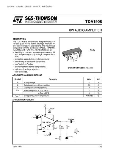
The TDA1908 is a monolithic integrated circuit in a 12‑lead quad‑in‑line package designed for low‑frequency power audio applications. It offers a flexible supply range of 4 V to 30 V, up to 3 A continuous output current, over‑temperature protection, soft limiting, and low noise operation.
The document details absolute maximum ratings, pin assignments, electrical characteristics, thermal data, and typical application circuits. Graphs illustrate quiescent output voltage, distortion, efficiency, bandwidth, and voltage gain across various supply voltages and loads. Mechanical dimensions of the package are also provided.
| Supply voltage range | 4 V to 30 V |
|---|---|
| Maximum output peak current (non‑repetitive) | 3.5 A |
| Maximum output peak current (repetitive) | 3 A |
| Power dissipation at Tamb = 80 °C | 1 W |
| Junction temperature range | -40 °C to 150 °C |
| Quiescent output voltage (Vs=4 V) | typical 2.1 V |
| Output stage saturation voltage (Ic=1 A) | 0.5 V |
| Small‑signal bandwidth (‑3 dB) | 40 kHz to 40 kHz |
| Open‑loop voltage gain (1 kHz) | 75 dB |
| Supply voltage rejection | ≈40 dB |
The TDA1908 can be operated up to 30 V supply voltage.
It can deliver up to 3.5 A non‑repetitive and 3 A repetitive output current.
Yes, the device has built‑in protection against chip overtemperature.