
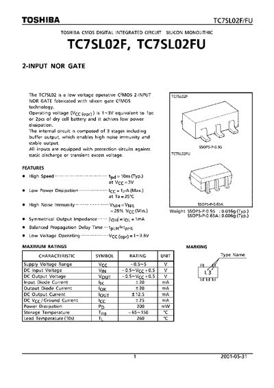
The TC7SLO2F/FU is a low‑voltage CMOS 2‑input NOR gate with high noise immunity and low power dissipation. It features a three‑stage internal circuit with buffered output and static‑discharge protection on all inputs.
The document lists the device's operating voltage range (1 V to 3.6 V), typical propagation delay of 10 ns at 3 V, power dissipation of 200 mW, and package options (SSOP5‑P‑0.95 and SSOP5‑P‑0.65A). Mechanical data such as weight (0.016 g typical) and storage temperature limits (‑65 °C to 150 °C) are also included.
| Operating voltage (Vcc) | 1~3.6 V |
|---|---|
| Typical propagation delay (tod) | 10 ns at Vcc = 3 V |
| Power dissipation (Pb) | 200 mW |
| Package weight (SSOP5‑P‑0.95) | 0.016 g (typ) |
| Storage temperature range | -65 °C to 150 °C |
The device operates from 1 V up to 3.6 V.
The typical propagation delay is 10 ns when Vcc is 3 V.
The device can be stored from –65 °C to 150 °C.