
This data sheet mainly introduces the features and characteristics of TDA21106 chip, including fast rise and fall time, capable of sinking more than 4A peak current, adjustable high side MOSFET gate drive voltage via PVCC pin for optimizing ON losses and gate drive losses, integrated bootstrap diode for reducing the part count etc.
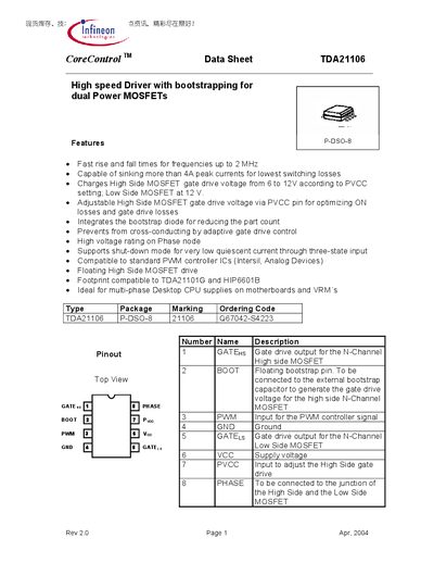
The TDA21106 is a dual high‑speed driver designed to drive N‑Channel low‑side and high‑side MOSFETs in half‑bridge configurations. It targets applications such as multi‑phase CPU supplies, VRM modules, motor drives, and Class‑D audio amplifiers, offering fast rise/fall times and low switching losses.
Key features include bootstrapped high‑side drive, adjustable high‑side gate voltage, integrated bootstrap diode, adaptive gate‑drive control, and a shutdown mode for low quiescent current. The device is supplied in a P‑DSO‑8 package and is pin‑compatible with TDA21101G and HIP6601B.
| Maximum switching frequency | up to 2 MHz |
|---|---|
| Peak sink current | more than 4 A |
| High‑side gate drive voltage range | 6 V to 12 V |
| Maximum duty cycle | 2 % |
| Operating temperature range | -55 °C to 150 °C |
The driver supports frequencies up to 2 MHz.
It can sink more than 4 A of peak current.
The high‑side gate drive voltage can be set between 6 V and 12 V.
The maximum duty cycle is limited to 2 %.