
The ICL7660S Super Voltage Converter is a monolithic CMOS voltage conversion IC that offers significant performance advantages over similar devices. It is a direct replacement for the industry standard ICL7660, with an extended operating supply voltage range up to 12V and lower supply current. The ICL7660S does not require an external diode. Additionally, a Frequency Boost pin allows for achieving lower output impedance using smaller capacitors. All improvements are detailed in the “Electrical Specifications” section on page 3. Critical parameters are guaranteed across commercial, industrial, and military temperature ranges. The ICL7660S performs positive to negative supply voltage conversion for an input range of 1.5V to 12V, resulting in complementary output voltages of -1.5V to -12V. Only 2 non-critical external capacitors are needed for the charge pump and charge reservoir functions. The ICL7660S can function as a voltage doubler, generating up to 22.8V with a 12V input. It can also be used as a voltage multiplier or voltage divider. The chip includes a series DC power supply regulator, RC oscillator, voltage level translator, and four output power MOS switches. The oscillator, when unloaded, oscillates at a nominal frequency of 10kHz for a 5.0V input supply voltage. This frequency can be lowered by adding an external capacitor.
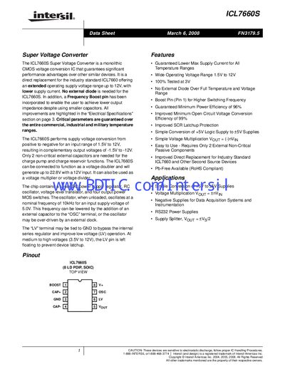
The ICL7660S Super Voltage Converter is a CMOS charge‑pump device that converts a positive supply (1.5 V to 12 V) into a complementary negative output (‑1.5 V to ‑12 V). It requires only two non‑critical external capacitors and eliminates the need for an external diode, offering improved efficiency and lower supply current compared with the standard ICL7660.
Key features include a boost pin that raises the oscillator frequency for lower output impedance, guaranteed minimum power efficiency of 96 %, voltage‑conversion efficiency of 99 %, and operation over a wide temperature range (‑40 °C to +85 °C). The device is available in Pb‑free, RoHS‑compliant PDIP and SOIC packages and is suited for negative‑voltage generation in data‑acquisition, instrumentation, and RS‑232 power‑supply applications.
| Input voltage range | 1.5 V – 12 V |
|---|---|
| Output voltage range | -1.5 V – -12 V |
| Minimum power efficiency | 96 % |
| Minimum voltage‑conversion efficiency | 99 % |
| Storage temperature range | -65 °C – +150 °C |
No external diode is needed for the ICL7660S.
The Boost pin (Pin 1) raises the switching frequency, which reduces output impedance.
Only two non‑critical external capacitors are needed for the charge‑pump operation.
Yes, the ICL7660S is available in a Pb‑free, RoHS‑compliant version.