
This datasheet provides detailed information about ATmega328P-P/R/U/X/U4/U8 microcontroller's pin functions, package types, pin layout, technical specifications, electrical characteristics, program memory and data memory, timers, comparators, serial interfaces, ADC, analog comparator, power management module, pin specifiers and exception vector table.
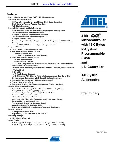
The ATtiny167 is a low‑power CMOS 8‑bit microcontroller based on Atmel's enhanced AVR RISC architecture. It offers up to 1 MIPS per MHz, a rich set of peripherals including LIN/UART, SPI, a 10‑bit ADC, watchdog timer, and multiple power‑saving modes, making it suitable for automotive and embedded applications.
The document provides a complete description of the device, including pin‑out diagrams for SOIC20, TSSOP20 and QFN32 packages, detailed register maps, CPU core architecture, electrical specifications, programming methods (ISP, parallel, serial), and typical application guidelines. It also lists ordering information, packaging options, and errata.
| Operating Voltage | 2.7 V – 5.5 V |
|---|---|
| Flash Memory | 16 KB In‑System Programmable Flash |
| EEPROM | 512 bytes |
| SRAM | 512 bytes |
| General‑purpose I/O lines | 6 |
| Programmable I/O lines | 16 |
| ADC | 10‑bit, 4‑channel |
| Package options | 20‑pin SOIC, 32‑pad QFN, 20‑pin TSSOP |
The device operates from 2.7 V to 5.5 V.
It includes 16 KB of In‑System Programmable Flash memory.
The microcontroller has six general‑purpose I/O lines and sixteen programmable I/O lines.
The ATtiny167 features a 10‑bit ADC with four selectable channels.