
This document is the datasheet of AD6623, which introduces the functions and features of the chip. The chip is a 4-channel, 104 MSPS digital transmit signal processor (TSP) that supports real or complex output and can be cascaded to increase the number of channels.
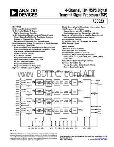
The AD6623 is a 4‑channel Transmit Signal Processor (TSP) that generates high‑bandwidth digital IF signals for transmit DACs. It features an 18‑bit parallel digital IF output, programmable RAM coefficient filters, and support for various modulation schemes such as QPSK, GMSK, and 8‑PSK. The device is pin‑compatible with the AD6622 and operates with a 2.5 V core supply and 3.3 V I/O.
Applications include cellular base stations, wireless local loop, multicarrier transmitters, phased‑array beam‑forming antennas, and software‑defined radio. The datasheet provides detailed electrical characteristics, timing specifications, pin configurations for both MQFP and CSPBGA packages, and guidelines for cascading multiple devices.
| Core supply voltage (VDD) | 2.5 V |
|---|---|
| I/O supply voltage (VDDIO) | 3.3 V |
| Logic "1" input voltage range | 2.0 V to 5.0 V |
| Logic "0" input voltage range | -0.3 V to 0.8 V |
| Maximum clock period | 9.6 ns |
| Operating temperature range | -40 °C to +85 °C |
The AD6623 requires a 2.5 V core supply voltage.
The I/O supply voltage (VDDIO) is 3.3 V.
Logic high ("1") voltage is specified from 2.0 V to 5.0 V.
The minimum clock period is 9.6 ns.