
This document describes the features and characteristics of the Super Sequencer and Monitor ADM1068 Rev.B. It is a complete supervisory and sequencing solution for up to 8 supplies, providing 8 supply fault detectors and 4 selectable input attenuators. It offers high accuracy and reliability.
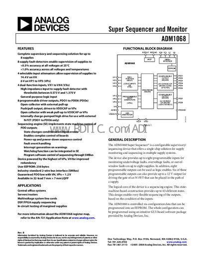
The ADM1068 Super Sequencer and Monitor is a configurable supervisory and sequencing device for up to eight supplies. It provides fault detection, programmable driver outputs, and an SMBus interface for configuration. The handbook details the device’s functional block diagram, pin assignments, and typical performance characteristics.
Key sections cover specifications, absolute maximum ratings, thermal resistance, ESD precautions, power supply requirements, and programming procedures for supply fault detectors. An ordering guide and package dimensions are also included.
| High‑Voltage Input Range (VH) | 3.0 V to 14.4 V |
|---|---|
| Low‑Voltage Input Range (VPx) | 3.0 V to 6.0 V |
| Supply Current (lv, Ivex) | 4.2 mA to 6 mA |
| EEPROM Erase Current | 10 mA (1 ms duration) |
| Maximum Voltage on VH Pin | 16 V |
| Maximum Junction Temperature | 150 °C |
| SMBus Clock Frequency | 400 kHz |
| Charge‑Pump Output Impedance (PDO1‑PDO6) | 500 kΩ |
The VH pin accepts voltages from 3.0 V to 14.4 V.
The device provides eight programmable driver outputs, labeled PDO1 to PDO8.
Configuration is performed via the industry‑standard 2‑wire SMBus interface.
Each PDO pin can tolerate up to 16 V.