
The AD ADC84/AD ADC85 series devices are high speed, low cost 12-bit successive approximation analog-to-digital converters that include an internal clock, reference, and comparator. Its hybrid IC design utilizes MSI digital and linear monolithic chips in co
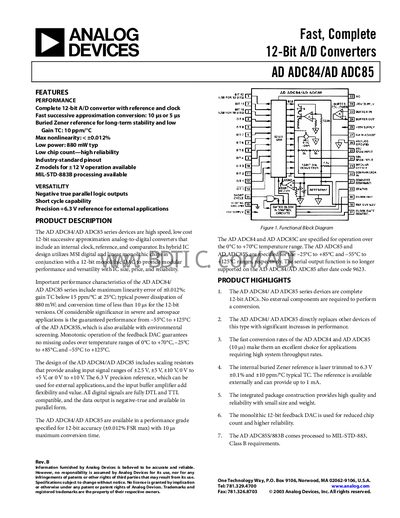
The AD ADC84 and AD ADC85 series are complete 12‑bit A/D converters that integrate reference, clock and comparator in a single IC. They provide fast successive‑approximation conversion (10 µs for 12‑bit) with low power consumption (≈880 mW) and a variety of input voltage ranges.
The devices feature negative‑true parallel digital outputs, DTL/TTL‑compatible inputs, and optional +12 V operation (Z models). They are offered in a DH‑32F ceramic DIP package and meet MIL‑STD‑883B processing requirements for aerospace and industrial applications.
| Resolution | 12 bits |
|---|---|
| Typical Power Dissipation | 880 mW |
| Reference Voltage | 6.3 V ±0.1 % (laser trimmed) |
Typical power dissipation is about 880 mW.
All digital inputs are fully DTL and TTL compatible.