
The ADADC80 is a 12-bit successive approximation integrated circuit ADC manufactured by Analog Devices. It has high precision, low power consumption, and fast conversion time.
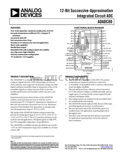
The ADADC80 is a complete 12‑bit successive‑approximation analog‑to‑digital converter that integrates an internal clock, reference, comparator and a monolithic DAC. It provides true 12‑bit operation, low power (800 mW), fast conversion (25 µs), and parallel digital output, making it suitable for high‑throughput applications.
The datasheet details specifications such as resolution, input voltage ranges, gain and offset errors, power‑supply sensitivity, and conversion speed. It also includes pin configuration, typical performance curves, theory of operation, and ordering information for the 32‑lead DIP package.
| Resolution | 12 Bits |
|---|---|
| Bipolar Input Voltage Range | +2.5 V, +5 V, +10 V |
| Gain Error (Bipolar) | +0.1 % of FSR |
| Linearity Error | +0.012 % of FSR |
| Power‑Supply Sensitivity (+15 V) | +0.0030 % of FSR/% Vs |
| Internal Reference Voltage | 6.3 V |
The ADADC80 provides a 12‑bit resolution.
It uses a precision internal reference of 6.3 V.