
This document introduces the features and characteristics of AD667 digital-to-analog converter, including complete 12-bit D/A function, double-buffered latch, high stability buried Zener reference, single-chip construction, guaranteed monotonicity and linearity over temperature range, guaranteed 3µs maximum conversion time and 0.01% maximum accuracy, support for -12V or -15V power supply, low power and TTL/5V CMOS compatible logic inputs
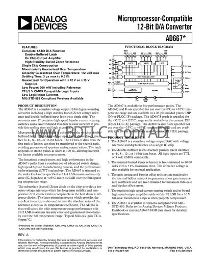
The AD667 is a complete 12‑bit digital‑to‑analog converter that integrates a high‑stability buried Zener voltage reference, double‑buffered input latch and on‑chip output amplifier on a single chip. It uses precision bipolar current‑steering switches and a laser‑trimmed resistor network to achieve fast settling and high linearity.
Four performance grades (A‑J‑K‑S) are offered in DIP, PLCC, LCC and ceramic packages, covering temperature ranges from –55 °C to +125 °C. The device provides TTL/5 V CMOS‑compatible logic inputs, low power consumption (≈300 mW), and optional MIL‑STD‑883‑qualified versions.
| Resolution | 12 bits |
|---|---|
| Logic Input Compatibility | TTL/5 V CMOS compatible |
| Settling Time | 3 ps max to 0.01 % FS |
| Supply Voltage | +12 V or +15 V |
| Gain Error (typ) | ±0.1 % FSR |
| Differential Linearity Drift | ±2 ppm/°C |
The AD667 settles to within 0.01 % of full scale in as little as 3 ps.
The device operates from either a +12 V or a +15 V supply.
The converter provides a 12‑bit resolution.