
This document introduces the ADF4150HV 3.0GHz high voltage fractional-N/integer-N frequency synthesizer, which has an integrated high voltage charge pump function and can be used in wireless infrastructure, microwave point-to-point/point-to-multipoint radios, VSAT radios, test equipment and private land mobile radios.
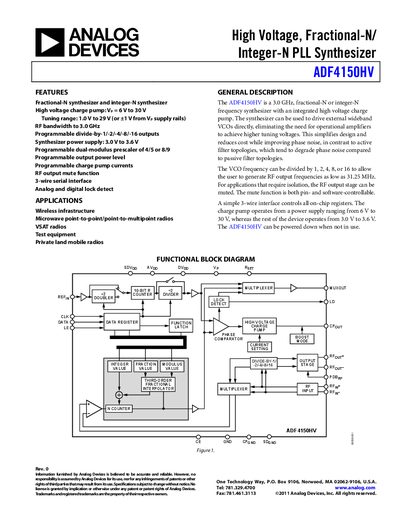
The ADF4150HV PLL synthesizer integrates a high‑voltage charge pump (6 V to 30 V) and supports both fractional‑N and integer‑N modes. It offers programmable output dividers (÷1, ÷2, ÷4, ÷8, ÷16) to generate RF outputs from 31.25 MHz up to 500 MHz, a 3‑wire SPI‑compatible serial interface, and a mute function controllable by the PDB RF pin.
The datasheet provides detailed specifications, timing diagrams, pin configurations, typical performance curves, PCB design guidelines for the chip‑scale package, and application notes for wireless infrastructure, microwave links, and test equipment.
| Input Frequency Range | 10 MHz – 300 MHz |
|---|---|
| High‑Voltage Charge Pump Supply (V P) | 6 V to 30 V |
| Core Power Supply (AV DD) | 3.0 V – 3.6 V |
| Operating Temperature Range | −40 °C to +85 °C |
| RF Output Frequency Range (with dividers) | 31.25 MHz – 500 MHz |
| RF Input Power Range | −10 dBm to +5 dBm |
The charge pump operates from 6 V up to 30 V.
Driving the PDB RF pin low mutes the RF outputs; this can also be controlled by software.
It operates from –40 °C to +85 °C.
A 3‑wire serial (SPI‑compatible) interface using CLK, DATA and LE pins.