
This document is about ADF4351 technical data. The chip is a wideband synthesizer with integrated VCO, supporting 35MHz to 4400MHz output frequency range, supporting fractional-N and integer-N frequency synthesis, low phase noise output, programmable prescaler and output power level, 3-wire serial interface, analog and digital lock detection, switched bandwidth fast-lock mode and cycle slip reduction.
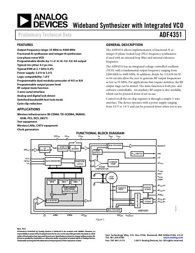
The ADF4351 is a wideband frequency synthesizer that integrates a voltage‑controlled oscillator (VCO) and supports both fractional‑N and integer‑N PLL operation. It offers an output frequency range from 35 MHz to 4.4 GHz, with a fundamental VCO range of 2.2 GHz to 4.4 GHz, and includes programmable divide‑by circuits, a fast‑lock mode, and an RF mute function.
The document provides detailed specifications, pin configurations, timing characteristics, absolute maximum ratings, and typical performance graphs. It also describes the internal architecture, register maps, and example circuits for implementing the device in wireless infrastructure, test equipment, and other RF applications.
| Output frequency range | 35 MHz to 4400 MHz |
|---|---|
| Fundamental VCO frequency range | 2200 MHz to 4400 MHz |
| Power supply voltage | 3.0 V to 3.6 V |
| Operating temperature range | -40 °C to +85 °C |
| Typical RMS jitter | 0.3 ps rms |
| Phase‑noise at 10 kHz offset (2.2 GHz) | -89 dBc/Hz |
The device can generate RF output frequencies from 35 MHz up to 4.4 GHz.
It operates from a 3.0 V to 3.6 V analog power supply.
The part is rated for –40 °C to +85 °C operation.
Pin 26 (PDB) disables the RF output when driven low.