
The MAX2306/MAX2308/MAX2309 are IF receivers designed for dual-band, dual-mode, and single-mode N-CDMA and W-CDMA cellular phone systems. The signal path consists of a variable-gain amplifier (VGA) and I/Q demodulator. The devices feature guaranteed +2.7V operation, a gain control range of over 110dB, and high input IP3 (-31dBm at 35dB gain, 3.4dBm at -35dB gain). Unlike similar devices, the MAX2306 family of receivers includes dual oscillators and synthesizers to form a self-contained IF subsystem. The synthesizer’s refer- ence and RF dividers are fully programmable through a 3-wire serial bus, enabling dual-band system architec- tures using any common reference and IF frequency. The differential baseband outputs have enough band- width to suit both N-CDMA and W-CDMA systems, and offer saturated output levels of 2.7Vp-p at a low +2.75V supply voltage. Including the low-noise voltage-con- trolled oscillator (VCO) and synthesizer, the MAX2306 draws only 26mA from a +2.75V supply in CDMA (dif- ferential IF) mode. The MAX2306/MAX2308/MAX2309 are available in 28- pin Thin QFN and QFN packages.
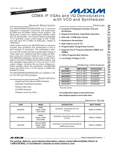
The MAX2306, MAX2308, and MAX2309 are IF receivers designed for dual‑band, dual‑mode and single‑mode CDMA and W‑CDMA cellular phone systems. Each device includes a variable‑gain amplifier (VGA), quadrature demodulator, VCO and programmable synthesizer, all powered from a low‑voltage +2.7 V supply.
The chips are supplied in 28‑pin thin‑QFN packages, support input frequencies from 40 MHz to 300 MHz, and provide a saturated output level of 2.7 Vp‑p. Programming is performed via a 3‑wire serial interface, allowing full control of gain, charge‑pump current, and synthesizer settings.
| Supply Voltage (VCC) | +2.7 V to +5.5 V |
|---|---|
| Gain Control Range | >110 dB |
| Saturated Output Level | 2.7 Vp‑p |
| Supply Current (CDMA mode) | 26 mA |
| Package | 28‑pin Thin QFN |
| Operating Temperature Range | -40 °C to +85 °C |
The devices operate from +2.7 V up to +5.5 V.
The variable‑gain amplifier offers a gain control range of more than 110 dB.
The chip draws about 26 mA from a +2.75 V supply in CDMA mode.