
The DS4M125/DS4M133/DS4M200 are margining clock oscillators with LVPECL or LVDS outputs. They are designed to fit in a 5mm x 3.2mm ceramic package with an AT-cut fundamental-mode crystal to form a complete clock oscillator. The circuit can generate the following frequencies and their ±5% frequency deviations: 125MHz, 133.33MHz, and 200MHz. The DS4M125/ DS4M133/DS4M200 employ a low-jitter PLL to generate the frequencies. The typical phase jitter is less than 0.9ps RMS from 12kHz to 20MHz. Frequency margining is a circuit operation to change the output frequency to 5% higher or 5% lower than the nominal frequency. Frequency margining is accom- plished through the margining select pin, MS. This three-state input pin accepts a three-level voltage signal to control the output frequency. In a low-level state, the output frequency is set to the nominal frequency. When set to a high-level state, the frequency output is set to the nominal frequency plus 5%. When set to the mid- level state, the frequency output is equal to the nominal frequency minus 5%. If left open, the MS pin is pulled low by an internal 100kΩ (nominal) pulldown resistor. The DS4M125/DS4M133/DS4M200 are available with either an LVPECL or LVDS output. The output can be disabled by pulling the OE pin low. When disabled, both OUTP and OUTN levels of the LVPECL driver go to the LVPECL bias voltage, while the output of the LVDS driver is a logical one. The OE input is an active-high logic signal and
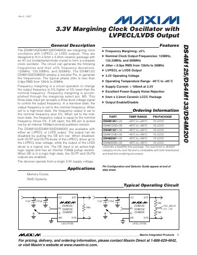
The DS4M125, DS4M133, and DS4M200 are compact 5 mm × 3.2 mm ceramic oscillators that operate from a single 3.3 V supply. They provide nominal clock frequencies of 125 MHz, 133.33 MHz, or 200 MHz with a ±5 % margining capability controlled by a three‑state MS pin. Both LVPECL and LVDS output options are available, and the output can be enabled or disabled via the OE pin.
Typical performance includes phase jitter below 0.9 ps RMS (12 kHz–20 MHz), supply current under 100 mA, and an operating temperature range of –40 °C to +85 °C. Detailed electrical characteristics, pin descriptions, and timing diagrams are provided for design integration.
| Nominal Clock Output Frequencies | 125 MHz, 133.33 MHz, 200 MHz |
|---|---|
| Supply Current | < 100 mA at 3.3 V |
| Operating Temperature Range | -40 °C to +85 °C |
Typical phase jitter is less than 0.9 ps RMS from 12 kHz to 20 MHz.