
This document describes the features and characteristics of the Toshiba CMOS digital integrated circuit TC7SG126FE Bus Buffer with 3-STATE Output, including high output current, ultra high-speed operation, 5.5V tolerant function on input terminals, and 3.6V power down protection function on output terminals.
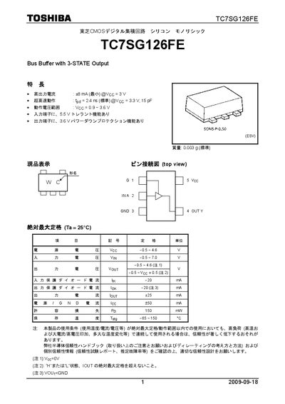
The TC7SG126FE is a 3‑state bus buffer from Toshiba, offering high output current and ultra‑fast switching. It operates over a wide supply voltage range and includes input over‑voltage and output power‑down protection features.
The datasheet provides detailed DC and AC electrical characteristics, pin configuration, package dimensions, and handling guidelines for reliable integration into electronic designs. This manual is written in Japanese.
| High output current | ≥8 mA (minimum) @ Vcc = 3 V |
|---|---|
| Propagation delay (tpd) | 2.4 ns (typ) @ Vcc = 3.3 V, 15 pF |
| Operating voltage range | 0.9 V – 3.6 V |
| Input voltage (VN) | 0 V – 5.5 V |
| Output current (Iout) | 25 mA |
| Supply/GND current (Icc) | ≤50 mA |
| Power dissipation (Pp) | 150 mW |
| Storage temperature | -65 °C – 150 °C |
| Input protection diode current (I_k) | -20 mA |
| Output protection diode current (I_ok) | -20 mA |
The device can source up to 25 mA of output current.
It operates with a supply voltage from 0.9 V to 3.6 V.
The typical propagation delay is 2.4 ns at Vcc = 3.3 V with a 15 pF load.
The part is rated for a maximum power dissipation of 150 mW.