
This document introduces Toshiba's CMOS digital integrated circuit, which features high-speed operation, low power consumption, high noise tolerance, high fanout, symmetrical output impedance, and wide operating voltage range.
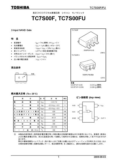
The TC7S00F/FU is a CMOS 2‑input NAND gate designed for high‑speed operation (7 ns typical propagation delay at 5 V) and ultra‑low standby current (1 nA max). It supports a wide supply range of 2 V to 6 V and can drive up to five LSTTL loads directly. The device offers balanced rise/fall times, high noise immunity, and a compact SSOP5 package.
The datasheet lists absolute maximum ratings, DC and AC electrical characteristics, pin configuration, and mechanical dimensions for both SSOP5‑P‑0.95 and SSOP5‑P‑0.65A packages. It also includes handling notices and reliability guidelines for designers. This manual is written in Japanese.
| Typical propagation delay | 7 ns @ Vcc=5 V |
|---|---|
| Supply current (standby) | 1 nA max @ Ta=25 °C |
| Supply voltage range | 2.0 V – 6.0 V |
| Maximum output current | 12.5 mA |
| Power dissipation | 200 mW |
| Operating temperature range | -65 °C to 150 °C |
| Package type | SSOP5‑P‑0.95 (0.016 g) or SSOP5‑P‑0.65A (0.006 g) |
The device operates from 2.0 V to 6.0 V.
Typical propagation delay is 7 ns at a 5 V supply.
The maximum output current is 12.5 mA.
It is offered in SSOP5‑P‑0.95 and SSOP5‑P‑0.65A packages.