
TC7SH07FE is a non-inverting (open drain) produced by Toshiba, which has the characteristics of high speed, low power consumption, and wide operating voltage range.
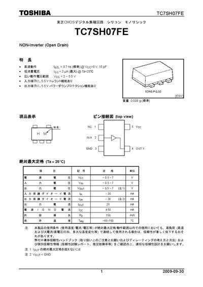
The TC7SH07FE is a CMOS digital integrated circuit featuring a non‑inverting (open‑drain) output. It offers high‑speed operation, low supply current, a wide operating voltage range, and built‑in input‑tolerant and output‑power‑down protection functions.
The document lists absolute maximum ratings, logic diagrams, DC and AC characteristics, package dimensions, and product handling recommendations to ensure reliable use in various electronic applications. This manual is written in Japanese.
| Propagation delay (typ) | 3.7 ns |
|---|---|
| Supply voltage range | 2–5.5 V |
| Input voltage range | -0.5–5 V |
| Output current (max) | 25 mA |
The absolute maximum rating for Vcc is –0.5 V to 7 V.
Typical propagation delay is 3.7 ns at Vcc = 5 V with a 15 pF load.
The device is specified to operate from –40 °C to 85 °C.
It is supplied in a SON5‑P‑0.50 package (approximately 1.6 mm × 0.5 mm).