
The TC74VHC595 is an advanced high speed 8-bit shift register/latch fabricated with silicon gate C2MOS technology. It achieves high speed operation similar to equivalent bipolar Schottky TTL while maintaining low power dissipation. The TC74VHC595 contains an 8-bit static shift register which feeds an 8-bit storage register. Shift operation is accomplished on the positive going transition of the SCK input. The output register is loaded with the contents of the shift register on the positive going transition of the RCK input. Since RCK and SCK signals are independent, parallel outputs can be held stable during the shift operation. And, since the parallel outputs are 3-state, they can be directly connected to an 8-bit bus. This register can be used in serial-to-parallel conversion, data receivers, etc. An input protection circuit ensures that 0 to 5.5V can be applied to the input pins without regard to the supply voltage. This device can be used to interface 5V to 3V systems and two supply systems such as battery backup. This circuit prevents device destruction due to mismatched supply and input voltages.
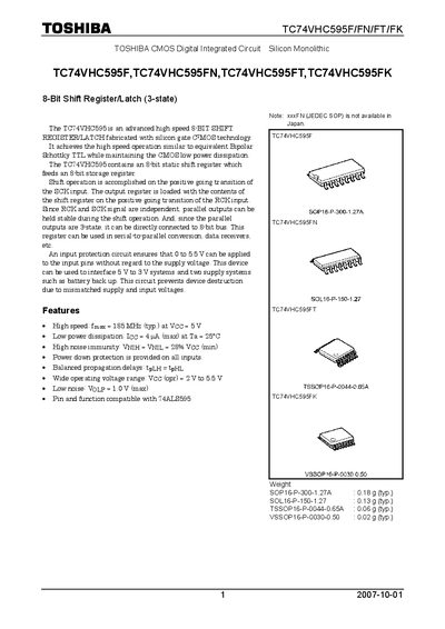
The TC74VHC595F is an 8‑bit shift register/latch fabricated with silicon gate C2MOS technology. It offers high‑speed operation comparable to bipolar Schottky TTL while maintaining low CMOS power dissipation, and features 3‑state parallel outputs suitable for bus interfacing and serial‑to‑parallel conversion.
The document details electrical characteristics, absolute maximum ratings, timing requirements, package dimensions, and usage restrictions. Key parameters include a typical fmax of 185 MHz, supply voltage range of 2 V to 5.5 V, and a power dissipation limit of 180 mW. Pin assignments, truth tables, and timing charts are provided for design integration.
| Maximum operating frequency | 185 MHz (typ.) at Vcc = 5 V |
|---|---|
| Supply voltage range | 2 V to 5.5 V |
| Quiescent current | 4 µA (max) at 25 °C |
| Power dissipation (absolute max) | 180 mW |
| Package weight (SOP16) | 0.18 g (typ.) |
The device can operate up to a typical 185 MHz at a 5 V supply.
It operates with a supply voltage from 2 V to 5.5 V.
The typical quiescent current is 4 µA (maximum) at 25 °C.
The absolute maximum power dissipation is 180 mW.