
This document describes the features and characteristics of the Toshiba CMOS Digital Integrated Circuit Silicon Monolithic TC7SZ32F, TC7SZ32FU 2-Input OR Gate released on September 9, 2009.
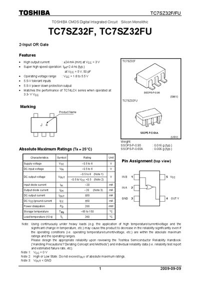
The Toshiba TC7SZ32F/FU is a 2‑input OR gate offering high output current (+24 mA min at V OC = 3 V) and super‑high speed operation (typical propagation delay 2.4 ns at V CC = 5 V, 50 pF). It operates over a supply voltage range of 1.8 V to 5.5 V and features 5.5‑V tolerant inputs with power‑down protection.
The document provides detailed electrical specifications, AC characteristics, package dimensions for SSOP5‑P‑0.95 and SSOP5‑P‑0.65A variants, and extensive usage restrictions covering safety, reliability and export compliance.
| High output current | +24 mA (min) at V OC = 3 V |
|---|---|
| Propagation delay | 2.4 ns (typ.) at V CC = 5 V, 50 pF |
| Supply voltage range | 1.8 V to 5.5 V |
| Operating temperature | -40 °C to 85 °C |
| Power dissipation | 200 mW |
| Package weight (SSOP5‑P‑0.95) | 0.016 g (typ.) |
The device operates with a supply voltage from 1.8 V to 5.5 V.
Typical propagation delay is 2.4 ns at V CC = 5 V with a 50 pF load.
The maximum power dissipation is 200 mW.
Yes, the document lists restrictions including prohibited uses in high‑risk applications, export controls, and safety compliance requirements.