
Key facts
- Brand
- STMicroelectronics
- Model
- STB75NF75L
- Industry
- Industrial
- Documents
- 2
- Languages
- EN
- Last added
- 2012-04-01
Start here
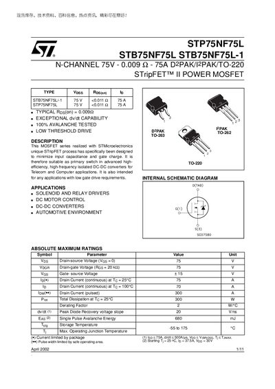
ST STP75NF75L STB75NF75L STB75NF75L-1 Manual(1)
This datasheet describes the STP75NF75L (and its STB75NF75L variant) N‑channel power MOSFETs. It lists the key electrical characteristics, including voltage ratings, current capability, on‑resistance and switching parameters, as well as thermal limits and package options such as D2PAK, I2PAK and TO‑220.
The document also contains mechanical dimensions, footprint data, and recommended test circuits for evaluating performance in applications like solenoid drivers, DC‑motor control, DC‑DC converters and automotive environments.
STMicroelectronics STB75NF75L specifications
| Drain‑source Voltage (Vds) | 75 V |
|---|---|
| Continuous Drain Current (Id) @ 25 °C | 75 A |
| Pulsed Drain Current (Id) (max) | 300 A |
| Typical On‑Resistance (Rds(on)) | 0.009 Ω |
| Package Types | D2PAK / I2PAK / TO‑220 |
| Thermal Resistance Junction‑case (RθJC) | 0.5 °C/W (max) |
| Storage Temperature Range | 55 °C to 175 °C |
All STMicroelectronics STB75NF75L documents by type
Ratings, dimensions and ordering codes, for selection and design work.
Questions answered in these manuals
What is the maximum drain‑source voltage for the STP75NF75L MOSFET?
The device is rated for a maximum drain‑source voltage of 75 V.
What is the typical on‑resistance of the STP75NF75L?
Its typical on‑resistance is 0.009 Ω.
What is the maximum continuous drain current at 25 °C?
The MOSFET can handle a continuous drain current of 75 A at 25 °C.
What is the typical on‑resistance of the device?
The typical on‑resistance is 0.009 Ω.