
This manual describes the KAI-1003 Imager Evaluation Board, its architecture, operational settings, and connector assignments for use with a Timing…
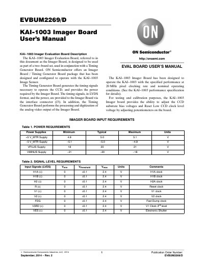
The KAI-1003 Imager Evaluation Board is designed to operate the KAI-1003 Image Sensor as part of a two-board set with a Timing Generator Board. The board provides the necessary power and timing signals to the CCD sensor and processes the analog video output. It allows for testing and calibration by adjusting CCD substrate bias voltages and Reset Low CCD clock level voltage via potentiometers on the board.
The document details the board's architecture, including power filtering, LVDS receivers, CCD pixel-rate clock drivers, and line drivers. It specifies input requirements for power and signal levels, operational settings for bias and clock voltages, and provides a comprehensive pinout for the interface connector.
| Pixel Clocking Rate | 20 MHz |
|---|---|
| +5 V_MTR Supply Min | 4.9 V |
| VPLUS Supply Max | 21 V |
| Output Amplifier Supply Nominal | 15.0 V |
| Line Driver Gain | 1.25 |
It is designed to be used as part of a two-board set with a Timing Generator Board to operate the KAI-1003 Image Sensor.
Coaxial cable with a characteristic impedance of 75 ohms should be used.