
TL494 is a fixed frequency, pulse width modulation control circuit designed primarily for SWITCHMODE power supply control. It features complete pulse width modulation control circuitry, on-chip oscillator, on-chip error amplifiers, on-chip 5.0 V reference, adjustable deadtime control, uncommitted output transistors rated to 500 mA source or sink, output control for push-pull or single-ended operation, undervoltage lockout, and NCV prefix for automotive and other applications requiring site and control changes.
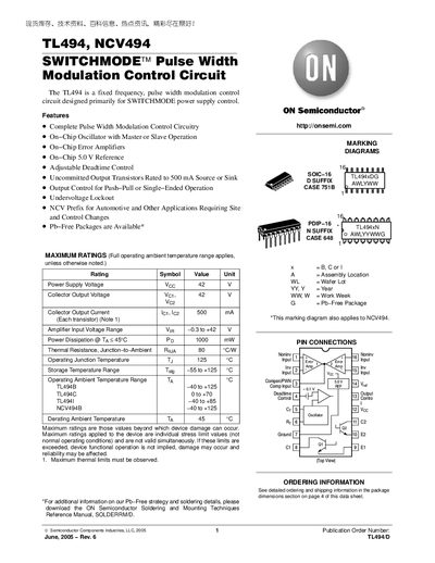
The TL494 and NCV494 are fixed‑frequency pulse‑width‑modulation control circuits designed for switching‑mode power‑supply applications. The datasheet provides complete electrical characteristics, maximum ratings, recommended operating conditions and functional block diagrams.
The document also lists available package types (SOIC‑16, PDIP‑16), ordering codes, mechanical dimensions and legal disclaimer information for automotive‑grade (NCV) and standard versions of the device.
| Power Supply Voltage (Voc) | 42 V |
|---|---|
| Collector Output Voltage (Voe) | 42 V |
| Collector Output Current (per transistor) | 500 mA |
| Power Dissipation (Pp) at 45 °C | 1000 mW |
| Thermal Resistance, Junction‑to‑Ambient (RθJA) | 80 °C/W |
| Maximum Operating Junction Temperature (Tj) | 125 °C |
| Storage Temperature Range | -55 °C to +125 °C |
Each output transistor can handle up to 500 mA of current.
The oscillator frequency can be programmed from 1 kHz up to 200 kHz using external timing components.
The recommended power‑supply voltage is between 7 V and 40 V.