
Technical datasheet for the JCS7N65B N‑channel MOSFET by Jilin Sino‑microelectronics, detailing ratings, electrical characteristics and packaging.
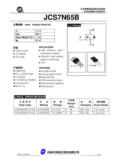
The JCS7N65B is an N‑channel enhancement‑mode MOSFET designed for high‑frequency switching power supplies, electronic lamp ballasts and UPS applications. It offers a 650 V drain‑source rating, low gate charge (25 nC) and fast switching performance while meeting RoHS requirements.
This datasheet provides absolute maximum ratings, detailed electrical parameters such as on‑resistance, gate charge and capacitances, thermal characteristics, mechanical dimensions for TO‑220C and TO‑220MF packages, and ordering information. Designers can use the curves and tables to verify suitability for their circuits. This manual is written in Chinese.
| Drain‑Source Voltage (VDSS) | 650 V |
|---|---|
| Total Gate Charge (Qg) | 25 nC |
| Operating Temperature Range | -55 °C to +150 °C |
The device is rated for a maximum drain‑source voltage of 650 V.
The MOSFET can operate from –55 °C up to +150 °C.