
Technical data sheet for the JT050N065WED N‑Channel IGBT, including ratings, electrical characteristics and thermal specifications.
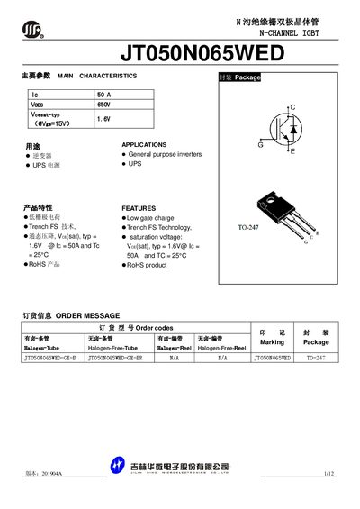
The JT050N065WED is a N‑channel insulated‑gate bipolar transistor (IGBT) offered in a TO‑247 package. It is intended for use in general‑purpose inverters and UPS power supplies, featuring low gate charge and trench‑FS technology.
The datasheet provides absolute maximum ratings, detailed electrical and switching characteristics, thermal resistance values, and mechanical dimensions, along with ordering information and safety notes from Jilin Sino‑Microelectronics.
| Collector‑Emitter Voltage (VCE) | 650 V |
|---|---|
| Continuous Collector Current (Ic) | 50 A |
| Pulse Collector Current (ICM) | 200 A |
| Power Dissipation (PD) | 437 W |
| Operating Temperature Range | -55 °C to +175 °C |
| Thermal Resistance Junction‑to‑Case (Rth(j‑c)) | 0.343 °C/W |
| Thermal Resistance Junction‑to‑Ambient (Rth(j‑A)) | 34.72 °C/W |
| Typical Saturation Voltage (VCE(sat)) | 1.6 V @ Ic=50 A, VGE=15 V |
| Total Gate Charge (Qg) | 121 nC |
| Turn‑Off Delay (td(off)) | 134 ns |
The device is rated for a maximum collector‑emitter voltage of 650 V.
At a collector current of 50 A and VGE = 15 V, the typical saturation voltage is 1.6 V.
It can operate from –55 °C up to +175 °C.
The maximum pulse collector current is specified as 200 A.