
The JCS7N65F N‑Channel MOSFET datasheet provides electrical characteristics, absolute maximum ratings, and mechanical data for design use.
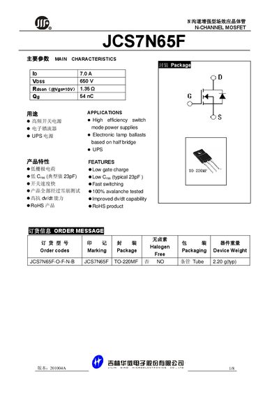
The JCS7N65F is a high‑frequency, low‑gate‑charge N‑Channel MOSFET intended for switch‑mode power supplies, electronic lamp ballasts, and UPS applications. The document lists its main characteristics, absolute ratings, and detailed electrical parameters.
Key specifications include a 650 V drain‑source voltage, 7 A continuous drain current, 1.35 Ω typical on‑resistance, and a total gate charge of 54 nC. Mechanical information such as the TO‑220MF package and a typical weight of 2.20 g are also provided, along with ordering codes and contact details for Jilin Sino-microelectronics.
| Drain‑Source Voltage (VDSS) | 650 V |
|---|---|
| Maximum Pulse Drain Current (IDM) | 28 A |
| Input Capacitance (Ciss) | 1380 – 1800 pF |
| Turn‑On Delay Time (td(on)) | 30 – 70 ns |
| Package | TO‑220MF |
| Device Weight | 2.20 g (typ) |
The device is rated for a maximum drain‑source voltage of 650 V.