
The document describes the features and characteristics of STP16NB25 and STP16NB25FP products. These products are designed using the latest high voltage MESH OVERLAY process and offer outstanding performance. They have extremely high dv/dt capability, are 100% avalanche tested, have very low intrinsic capacitances, and minimized gate charge.
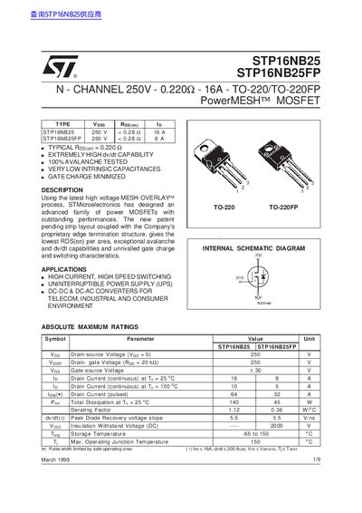
The STP16NB25/FP is a high‑voltage N‑channel PowerMESH MOSFET designed for high‑current, high‑speed switching applications such as UPS, DC‑DC and DC‑AC converters. The device features a low on‑resistance, high avalanche capability, and fast dv/dt performance.
The datasheet lists absolute maximum ratings, thermal resistance values, avalanche characteristics, detailed electrical parameters (VDS, ID, RDS(on), gate charge), switching timings, and mechanical dimensions for both TO‑220 and TO‑220FP packages.
| Drain‑source voltage (VDS) | 250 V |
|---|---|
| On‑resistance (RDS(on)) typical | 0.22 Ω |
The MOSFET can withstand up to 250 V between drain and source.
The typical RDS(on) is 0.22 Ω when VGS = 10 V and ID = 8 A.