
This document is about SEARAY connector routing guide, which provides detailed information on PCB pad layout, routing recommendations, grounding patterns, pin spacing, via structure and so on.
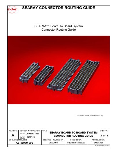
The SEARAY connector system is designed for mezzanine architectures in next-generation telecommunication and data networking equipment. It supports data rates up to 15 Gbps and offers high signal density with up to 67 differential pairs per inch. The system features an open pin field for flexible signal allocation and a recessed housing to protect terminals during mating.
| Data Rate | up to 15 Gbps |
|---|---|
| Signal Density | up to 67 differential pairs per inch |
| Circuit Sizes | 40 to 500 circuits |
| Stack Heights | 7 to 15mm |
| Solder Pad Diameter | .025" (0.635mm) |
| Recommended Trace Geometry | 5-5-5 mil |
| Max Differential Pair Width | 15 mils |
A 5-5-5 mil trace geometry is recommended within the via pin field for high-speed applications.
The system is designed for .025" (0.635mm) diameter solder pads.
It is recommended to route traces orthogonally to the differential pair directly through the pin field in a lateral escape configuration.