
This is 1760A description file.
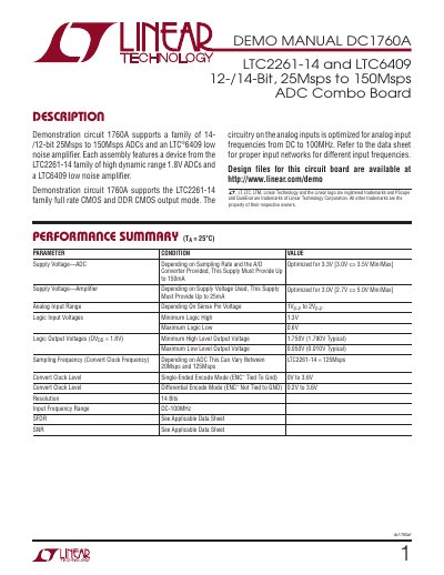
This document provides setup and operation instructions for the DC1760A demonstration circuit, which includes an LTC2261-14 ADC and LTC6409 amplifier. It covers jumper configurations, power requirements, analog input setup, and software configuration using PScope with DC890. The manual also details serial programming options for the ADC, including power modes, clock settings, and output modes.
The board supports both single-ended and differential input signals and requires specific filter networks for optimal performance. It is designed for evaluating ADC performance with proper clock and input signal conditioning.
| Supply Voltage—ADC | 3.3V [3.0V ⇔ 3.5V Min/Max] |
|---|---|
| Supply Voltage—Amplifier | 3.0V [2.7V ⇔ 5.0V Min/Max] |
| Analog Input Range | 1V P-P to 2V P-P |
| Logic Input Voltages | Minimum High 1.3V, Maximum Low 0.6V |
| Sampling Frequency | 20Msps to 125Msps |
| Resolution | 14 Bits |
| Input Frequency Range | DC-100MHz |
3.3V, with a range of 3.0V to 3.5V.
Minimum logic high is 1.3V and maximum logic low is 0.6V.
PScope software, which can be downloaded from Linear Technology’s website.
Full Rate (CMOS), Double LVDS, and Double CMOS (though Double CMOS is not supported by DC1760A).