
The document introduces the features and characteristics of Analog Devices' ADCLK854 low power clock fanout buffer. The product features selectable differential inputs, selectable LVDS/CMOS outputs, low power consumption, low jitter, etc. It is suitable for applications such as low jitter clock distribution, signal restoration, level translation, wireless communications, wired communications, medical and industrial imaging, ATE and high performance instrumentation.
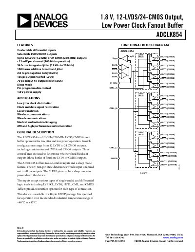
The ADCLK854 is a low power clock fanout buffer designed for low jitter and low power operation. It features two selectable differential inputs and can be configured to provide up to 12 LVDS outputs (up to 1.2 GHz) or 24 CMOS outputs (up to 250 MHz). The device includes a sleep mode for power management and accepts various input logic levels including LVPECL, LVDS, HSTL, CML, and CMOS.
The document provides comprehensive specifications, including electrical characteristics, timing parameters, and phase noise data for both LVDS and CMOS output modes. It also covers functional block diagrams, pin configurations, and application information for clock distribution and signal restoration.
| Input Frequency (Differential) | 1200 MHz |
|---|---|
| Output Frequency (LVDS) | 1200 MHz |
| Output Frequency (CMOS) | 250 MHz |
| Output Rise/Fall Time (LVDS) | 135 ps |
| Output Rise/Fall Time (CMOS) | 950 ps |
| Propagation Delay (LVDS) | 2.0 ns |
| Propagation Delay (CMOS) | 3.2 ns |
| Integrated Random Jitter (LVDS) | 54 fs rms |
| Integrated Random Jitter (CMOS) | 56 fs rms |
| Power Supply Voltage | 1.8 V |
The device supports up to 1200 MHz for LVDS outputs and 250 MHz for CMOS outputs.
Yes, the device includes a sleep mode feature to power down the unit.
The inputs accept LVPECL, LVDS, HSTL, CML, and CMOS logic levels.