
STMicroelectronics AN1214 Application Note Design Tips for L6561 PFC

This application note describes how to design a wide range PFC circuit.
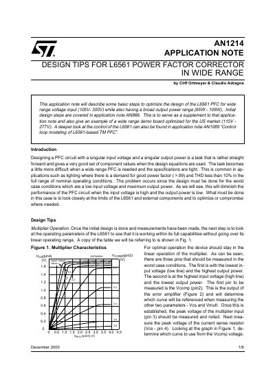

STMicroelectronics AN1214 Application Note Design Tips for L6561 PFC - cover page
Brand
STMicroelectronics
Document type
Application Note
Language
English
Pages
6
File format
PDF
File size
72 KB
Published
06 August, 2012
Updated
30 September, 2023
Model
L6561
MD5 checksum
F2FAEDA2614891AC47327A757EA53992

About this manual

This application note describes basic steps to optimize the design of the L6561 Power Factor Corrector (PFC) for a wide range of input voltages (105V-300V) and output power (65W - 105W). It serves as a supplement to application note AN966 and provides an example of a demo board optimized for the US market.

What's inside

  • Multiplier Operation
  • Zero crossing dead time
  • Input capacitance EMI filtering
  • Switching frequency
  • Step-gap core technique
  • Wide Range Example Circuit

Frequently asked questions

What input voltage range and output power range does this application note cover for the L6561?

The document describes optimizing the L6561 PFC for a wide range voltage input of 105V to 300V and a broad output power range of 65W to 105W.

What is the minimum recommended switching frequency for the L6561?

The text states that switching below 15kHz is not recommended because it may interfere with the internal starter.

What is the total primary inductance value for the example circuit transformer?

The example circuit specifies a gap of 1.25mm for a total primary inductance of 0.8mH.

Download PDF (72 KB)

More STMicroelectronics Manuals


View all STMicroelectronics manuals →