
How to use the TSM101 integrated circuit with a switching mode power supply (SMPS) to realize a battery charger
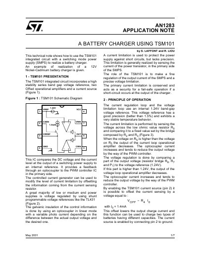
The document presents the TSM101 integrated circuit, which incorporates a high stability series band gap voltage reference, two ORed operational amplifiers, and a current source. It explains how the IC compares DC voltage and current levels at the output of a switching power supply to an internal reference, providing feedback through an optocoupler to a PWM controller IC on the primary side.
The note details the principle of operation, including current regulation and voltage limitation loops using an internal 1.24V band-gap voltage reference. It provides calculations for component selection, such as the sense resistor for current measurement and resistor bridges for voltage limitation. Additionally, it offers improvement suggestions, such as high frequency compensation, auxiliary winding power supply solutions, and methods for higher precision voltage control or variable charging currents based on cell voltage.
| Internal Voltage Reference | 1.24V |
|---|---|
| Voltage Reference Precision | better than 1.5% |
| Nominal Charge Current | 700mA |
| Low Current Mode | 200mA |
| End-of-Charge Voltage Limit | 1.45V/cell |
| Recommended Ambient Temperature | 25°C |
The charge current is regulated at 700mA if the charge control input is left open.
The charge current is reduced to 200mA if the charge control input is connected to ground.
The end-of-charge voltage is limited at 1.45V per cell for an ambient temperature of 25°C.
For medium currents less than 1A, a voltage drop of 200mV across the sense resistor is recommended.